Introduction
These are very exciting times: state-of-the-art technological developments are happening faster and faster. We are turning science fiction into reality. Earlier this month I travelled to Brussels to talk about one of the most important technological developments I have seen in my career: parallelism in automated photonic alignment.
New World
We all know our world is getting a lot smaller. We are manufacturing micro-electronic chips manufactured with nanoscale precisions. On top of that, the world has gotten a lot faster: massive data centers aggregate tens of thousands of computers to route information from one place to another in microseconds. All so that you and I can have a super computer in our pockets that provides us with all the information that can be found on the world wide web. Instantly.
However, energy saving is becoming a major issue as data centers scale up in size, capacity, and number. Together, the data centers in the United States already use more electricity than lighting. Every Google search you perform consumes a kilojoule of energy. Add up every light bulb and street light in the entire country and they will not use as much electricity as data centers. And demand for light bulbs isn’t growing exponentially! So, we’re reaching the limit of what can be sustainably achieved with conventional transistors and copper wires. What’s the next step?
Nanometers matter even more
Over the last couple of decades, we’ve seen a rise in the use of optical technologies. First came long-haul telecommunications, to replace satellite links with transoceanic and transcontinental optical connections, then regional and metropolitan links, and eventually fiber to the home. What we’re witnessing today is a continuation of that diminishing scale of photonic technology. Today we’re talking photonics on chips – Silicon Photonics.
This means that the technology can be applied to a great variety of fields and industries. We can now build sophisticated communications platforms out of microscopic lasers, detectors, or modulators. This lets computers in data centers transfer data using light, the way we have used electricity to convey information in the past.
Positioning challenge
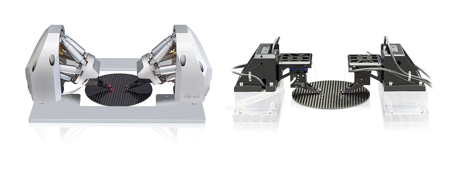
Optical fibers have more capacity, are faster, and use less energy than copper wires. The challenge, however, lies in the accuracy required to position optical fibers and other photonic elements with respect to each other so the light is efficiently coupled. The alignment must be correct down to the sub-micron or even nanometer scale. Often these devices are sensitive to angle, so that must be optimized too.
And then there are the multiple channels of array devices which all must be aligned. Sometimes these channels interact with each other, or their inputs and outputs steer each other, making the alignment a moving target! All in all, it can take a lot of time, effort, and money to reach the desired global consensus alignment. Until now.
Revolutionary algorithm
At PI, we have been able to create an entirely new technology that resides in our digital positioning controllers’ firmware, enabling manufacturers to accomplish all these complicated alignments at once – in one step. The key is the parallel execution of the alignment processes. We actually make it easy! This parallelism allows manufacturers to cost-effectively automate this complex process, ensuring their photonics production efforts provide high quality at low cost. Often, every channel and all degrees of freedom can be optimized with a single command.
This makes photonic alignment in manufacturing and testing extremely fast and adaptable to a variety of situations. It can be used for different operations, types of coupling, and devices. This is truly a revolutionary achievement because it makes the production of advanced photonic devices affordable, fast, sustainable, scalable, and green.
Newer World
At the Photonic Integrated Circuit conference in Brussels, I spoke about the new possibilities this groundbreaking technology enables. Some people had trouble believing what I was telling them, either from skepticism or because it seems impossible to align all these inputs, outputs, degrees of freedom, and channels in one go.
One engineer thought about what I’d presented overnight, and the next morning came to our booth to say: “I just don’t see how it is possible to do multiple alignments in one step in the general case.” Sure— it’s pretty hard to visualize, and the math is complicated!
Fortunately, we had taken the time to assemble an actual photonic array alignment demonstration in our booth, allowing attendees to come by to see multi-channel, multi-degree-of-freedom alignment processes running in parallel with their own eyes. The array alignment was complete in a couple of seconds, instead of several minutes as was required until now.
My main message at the conference? You better believe what you’re seeing because if your competitors recognize what is possible with this new technology and they implement it, you are going to be left behind. Luckily, I could see that my presentation and live demo convinced many delegates to take this significant development in the field of photonic process automation very seriously. It’s an enabler!