Motion and Control Solutions for Fast and Precise Positioning, Processing, and Testing of Electronic Components

Industry 4.0, 6G technologies, internet of things, cloud computing, autonomous driving, eHealth, or artificial intelligence benefit from advanced technology that the semiconductor and electronics industry are making available. At the same time, these growing markets are presenting them with great challenges: Even smaller components with better functionality, shorter innovation cycles, and a growing diversity of end products. Precision, throughput, reliability, and flexibility of production systems are becoming more decisive at a wafer and chip level, not to mention at printed circuit board level. Each positioning and motion task in the process must meet these requirements.

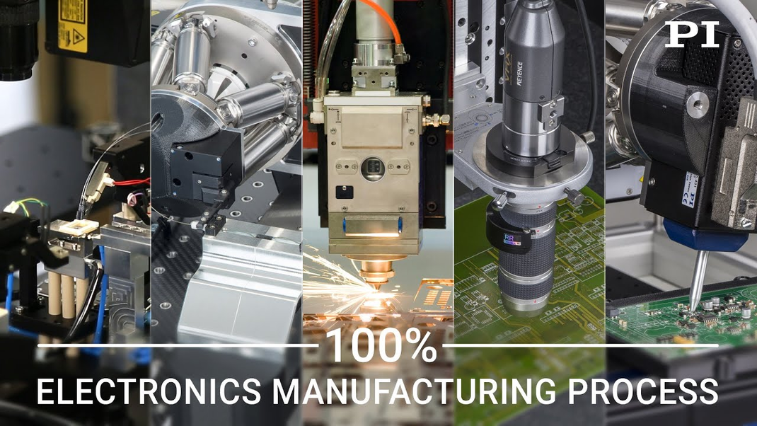
PI supports machine builders, integrators, and OEMs worldwide with positioning solutions to meet the required specifications for alignment, processing, or inspection. From the design phase, PI works with the manufacturers in order to select motion components so that, e.g., the assembly processes achieve the placement accuracy, work cycle, and throughput that is necessary for the next generation of electronics manufacturing.

PI is your partner for motion and control solutions for applications such as:

PCB manufacturing and assembly
Stencil production
Test probe cards manufacturing
Electronic devices testing
Printed electronics manufacturing
Inspection tools alignment
Enabling Higher Functional Density
Increasing the Functionality Density of Electronic Components
The printed circuit board (PCB) is the heart of any electrical device: Smartphone, smartwatch, tablet, industry electronics, electric car, camera and security systems, hearing aids, or pace makers – none of these technologies can do without it. It makes electronic devices come to life and makes trends in developments possible.
Learn more
Improving Quality in Stencil Production
Improving Speed and Cutting Quality in Stencil Production
Platform and motion control solutions for high-throughput and high-precision laser-based stencil production.
For the component assembly process, this means: A higher connection density, smaller connection surface, reduced installation space, more complex components, and a higher throughput.
Learn more
Driving Commercialization of a New Display Generation
A lighter and more flexible design, less energy consumption, higher resolution and even more contrast and brilliance. This is what future display technologies should achieve to meet the requirements for function, handling and lifetime. To make use of the potential of MicroLED technology and to enable economic mass production, PI supports research groups and manufacturers worldwide with drive, control and software solutions.
Learn more
Brochure

Motion Systems for Electronics Manufacturing

PLACE -> ALIGN -> PROCESS -> INSPECT -> TEST

Version / Date
BRO64E 2018-11
pdf - 9 MB
Version / Date
BRO64CN 2018-12
pdf - 15 MB

Learn more about a motion solution for testing electronic devices – presented by our expert

Do you have questions about our solutions? Our specialists are happy to help you!

Contact us today!